PG Diploma in VLSI Design
Advance your career to the highest level of business leadership. Transform your expertise into strategic impact with our globally recognized program.
Duration: 9 Months
Format: Online
Accredited Program
Apply Now
Start VLSI Today
Get Advice
Free Consultation
Download Brochure
Get Course Details
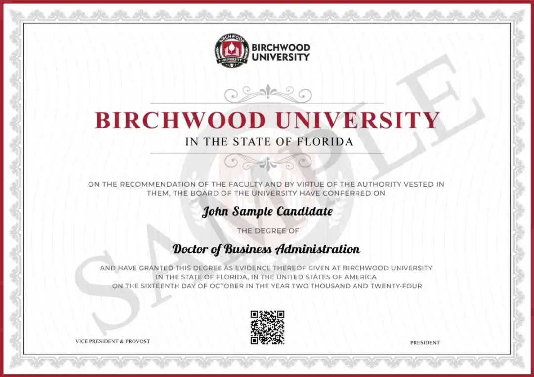


Doctor of Business Administration (DBA)
Advanced Your Career to the Highest Level of Business Leadership.
Duration: 2 Year
Format: Online
Accredited Program
Apply Now
Start DBA Today
Get Advice
Free Consultation
Download Brochure
Get Course Details
Course Overview
PG Diploma in VLSI Design
The PG Diploma in VLSI Design with Hands-On Chip Design Practice is an industry-focused program designed to equip learners with in-demand skills in integrated circuit design and semiconductor technologies. The program emphasizes practical learning, enabling participants to gain real-world experience in designing, simulating, and verifying digital and analog circuits used in modern electronic systems.
Learners receive hands-on training in VLSI fundamentals, digital and analog design, HDL programming, RTL design, verification, and physical design flows, using industry-standard tools and methodologies. The curriculum is structured to bridge the gap between academic knowledge and industry requirements, ensuring strong technical foundations and practical expertise.
The Changing Business Landscape
The Changing Business Landscape
The pace of change we are witnessing today is unlike anything we have seen in recent history.
75%
CEOs believe identifying the next generation of leaders is the most critical challenge facing organizations today.
$23.59B
Growth in the global business education market is fueled by rising adoption of advanced, career-focused qualifications.
40%
The demand for Doctor of Business Administration (DBA) professionals is projected to increase steadily until 2033.
$203,000
Median salary trends demonstrate the leadership impact and earning potential of qualified professionals.
Admission
Admission Requirements
General Admission Requirements
- A copy of a valid government-issued photo identity card.
- A copy of an updated resume.
- Any document if not in English must be accompanied by a certified translated copy.
Additional Admission Requirements for PG Diploma in VLSI Design
- Applicants applyingfor the PG Diploma in VLSI Design are expected to have completed or be in the final year of a Bachelor’s degree in Electronics, Electrical Engineering, Electronics & Communication Engineering (ECE), Instrumentation, Computer Engineering, or a closely related discipline from a recognized institution.
- Candidates should possess a basic understanding of digital electronics, semiconductor fundamentals, and circuit theory. Familiarity with HDL concepts (Verilog/VHDL), programming basics, or electronic design tools is desirable but not mandatory, as foundational concepts are covered during the program.
- Applicants must submit a completed application form, academic transcripts, an updated resume, and a valid government-issued photo identification. Academic documents not issued in English must be accompanied by a certified English translation.
Why Choose Us
Why choose PG Diploma in VLSI Design
The PG Diploma in VLSI Design is designed to prepare learners for the rapidly growing semiconductor and electronics industry. With increasing demand for advanced chips across sectors such as consumer electronics, automotive, telecommunications, and artificial intelligence, VLSI design skills have become highly valuable and future-ready. A PG Diploma in VLSI Design opens pathways to high-demand roles such as VLSI Design Engineer, ASIC Engineer, SoC Engineer, Verification Engineer, and Physical Design Engineer. With strong career growth, global opportunities, and competitive compensation, this program is ideal for graduates and working professionals seeking specialization in semiconductor and chip design technologies.
Objectives
Program Objectives
The PG Diploma in VLSI Design is designed to develop strong technical competence and practical expertise in integrated circuit and semiconductor design. The program aims to equip learners with in-depth knowledge of VLSI fundamentals, digital and analog circuit design, and modern chip design methodologies aligned with industry standards.
The program goals are:
- Goal 1: Build strong foundational knowledge in VLSI concepts, digital and analog circuit design, and semiconductor fundamentals.
- Goal 2: Develop practical skills in HDL programming, RTL design, simulation, and functional verification using industry-standard tools.
- Goal 3: Enable hands-on experience in ASIC and SoC design flows, including synthesis, timing analysis, and physical design.
- Goal 4: Strengthen analytical and problem-solving abilities for design optimization, performance improvement, and power efficiency.
- Goal 5: Prepare learners for industry-ready roles by applying VLSI design principles to real-world chip design projects and applications.
Licensure & Associations


Course Structure
Program Curriculum
1. RTL Design & Development Crash Course
- Introduction to VLSI
- Overview of Digital Logic Design
- Verilog HDL Design Techniques
- Lab Practice on Verilog
- Simple Project Implementation
2. RTL & FPGA Design Course
Duration: 6 Weeks
- Introduction to VLSI
- Details of Digital Logic Design
- Verilog HDL Full Design Techniques
- FPGA Full Design Techniques
- Lab Practice on Verilog
- Implementation on FPGA’s
- Real Time Project Implementation
3. RTL & FPGA With STA Design Course
Duration: 8 Weeks
- Introduction to VLSI
- Details of Digital Logic Design
- Verilog HDL Full Design Techniques
- FPGA Full Design Techniques
- Lab Practice on Verilog
- Implementation on FPGA’s
- Static Timing Analysis Details & Real Time Issues
- Real Time Project Implementation
4. RTL & SoC/ASIC Design Course
Duration: 12 Weeks
- Introduction to VLSI
- Details of Digital Logic Design
- Details of SoC Design Techniques
- Verilog HDL Full Design Techniques
- FPGA Full Design Techniques
- Lab Practice on Verilog
- Implementation on FPGA’s
- Implementation on SoC Based Tools
- Concepts of CDC
- Static Timing Analysis Details & Real Time Issues
- Real Time Project Implementation
5. Verilog - Design & Verification
Duration: 12 Weeks
- Introduction, Basic Programming Concept
- Verilog Modeling Style
- Register, Net
- Datatypes, Arrays, Vectors
- Operators
- Continuous Assignment
- Procedural Assignment
- Vector Operation
- Conditional Expression, always, if, case
- Loop Statement (while, for, foreach, do-while)
- Task, Function
- Generate Block
- Parameter, Macros
- Systemtask
- Module Instantiation
- Combinational Logic Modeling
- Sequential Logic Modeling
- FSM Modeling
- Memory Modeling
- Clock Modeling, Clock divider
- Timer
- Verilog File Handling
- TB Architecture
- Verification Environment Coding
- Testcase Bring-up
- Simulation Run
- Waveform Generation and Analysis
- Log File Analysis
- Simulation time data passing
- parameter override from TB
- randomization in Verilog
- seed passing
- Industrial Project Coding
6. Systemverilog (Basic + Advance)
Duration: 10 Weeks
- TB Architecture
- Data types, Array, Literals
- Operators
- Randomization, Constraint
- Class, OOPS
- Procedural Statements, Flow Controls fork-join, fork-join_any, fork-join_none, wait-fork, disable-fork
- Subroutines
- Struct, Union
- Systemtasks
- Interface, Modport, Clocking Block
- Event Scheduling
- Program Block
- Threads
- Interprocess Communication
- Virtual Interface
- Event Handling
- File Handling
- DPI
- Code Coverage and Functional Coverage
- Assertions
- TB Component Coding
- TB, TC Coding
- Stimulus Generation and Drive
- Simulation Run, Test Termination
- Error Debugging
- Log File and Waveform Analysis
- Industrial Project Coding
7. UVM (Basic + Advance)
Duration: 12 Weeks
- TB Architecture
- TLM
- Sequences and Items
- Sequencer, Driver, Monitor
- Env, Agent, Cov, Scoreboard, Test
- Build-in Methods
- UVM Configuration, Config DB
- Factory Override
- Callback
- UVM Event
- RAL
- project: AXI
8.Protocols
We are providing industrial protocol training for corporates,Institutes & Individuals.
Industrial protocol training such as:
USB,PCIe,AMBA BUS…etc
9. Projects
- Industry standard projects in Verilog,SV,UVM
10. LINUX Commands
LINUX Commands
11. Scripting
- Shell Script
- Perl Script
- Python Script
More Information
Additional Information for PG Diploma in VLSI Design
FAQs
Frequently Asked Questions
What are the basic requirements of the PG Diploma in VLSI Design at Birchwood University?
Applicants should hold a Bachelor’s degree (or be in the final year) in Electronics, Electrical/ECE, Computer Engineering, or a related field. An updated resume, valid photo ID, and academic documents are required. Prior VLSI experience is preferred but not mandatory.
Do I need to visit University campus during the course of the program?
No. The PG Diploma in VLSI Design at Birchwood University is delivered fully online, so you do not need to visit the campus. You’ll complete all coursework, labs, and assessments remotely to earn the diploma.
How long is the VLSI Design course that Birchwood University offers?How long is the VLSI Design course that Birchwood University offers?
The PG Diploma in VLSI Design at Birchwood University is a 9-month program. The flexible online structure allows learners to complete coursework and hands-on project work while balancing personal and professional commitments.
What career opportunities are available after the VLSI Design course?
- Graduates of the VLSI Design course can pursue a variety of career opportunities in the semiconductor and electronics industry. Common roles include VLSI Design Engineer, ASIC Engineer, SoC Engineer, Verification Engineer, Physical Design Engineer, RTL Design Engineer, and Semiconductor Design Engineer.
Is the VLSI Design Course at Birchwood University worth it?
Yes. The PG Diploma in VLSI Design at Birchwood University offers a comprehensive and industry-relevant curriculum focused on practical chip design skills and semiconductor technologies. With hands-on training, real-world project experience, and exposure to industry-standard tools, the program prepares learners for in-demand roles in VLSI and semiconductor engineering.
Begin Your Career Journey Today!
Your Career Starts Here, Take the first step
Apply now to take the first step in starting your career